Title:Dac Using PIC18F4520
Analog to Digital Converter (ADC) is a device that converts an analog quantity (continuous voltage) to discrete digital values. This is very useful when we want to do some processing on physical quantities, which are normally analog in nature. Most of the PIC Microcontrollers have built in ADC Module. Here we are using pic18f4520 for demonstrating the working.
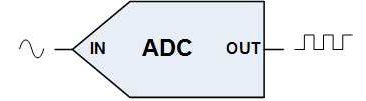
ADC_Symbol
ADC of PIC Microcontrollers have 5 inputs for 28 pin devices and 8 inputs for 40/44 pin devices. It is a 10-bit ADC, ie the conversion of analog signal results in corresponding 10-bit digital number. The positive and negative reference voltage (+Vref and -Vref) of PIC ADC is software selectable, which can be VDD, VSS, voltage at RA2 or RA3. This A/D Converter module can also operate in sleep mode in which clock is derived from its internal RC oscillator. Following points may help you to understand the concept of reference voltages.
- When the ADC input is -Vref, result will be 0000000000
- When the ADC input is +Vref, result will be 1111111111
- Resolution of ADC = (+Vref – -Vref)/(210 – 1), which is the minimum voltage required to change the ADC result by one bit.
We require some hardware knowledge to program PIC ADC in Hi-Tech C. If you don’t need hardware knowledge please skip this part and go to Circuit Diagram.
ADC Module in Detail
Registers
PIC ADC has 4 registers :
- ADCON0 – ADC Control Register 0
- ADCON1 – ADC Control Register 1
- ADRESH – ADC Result High Register
- ADRESL – ADC Result Low Register
ADCON0 Register
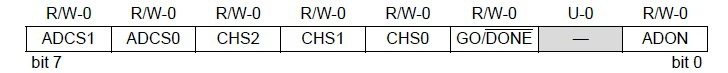
ADCON0 Register – PIC 16F877A
- ADCS1 and ADCS2 are used to select A/D Conversion Clock. It should be selected in accordance with device clock.
- CH2, CH1 and CH0 are used to select one of the analog input channel out of eight channels.
- GO/DONE is the A/D Conversion Status bit. Setting this bit initializes A/D Conversion and will be automatically cleared when the conversion is complete.
- ADON is used to switch on/off the ADC Module. When it is 1, the ADC Module turns ON and when it is 0, the ADC Module will be OFF.
ADCON1 Register
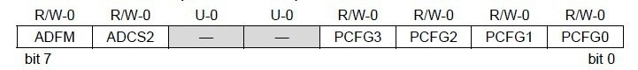
ADCON1 Register – PIC 16F877A
- ADFM is the ADC Result Format select bit. Two 8 bit register (ADRESH and ADRESL) are provided to store the 10-bit result of A/D Conversion, thus we need’t use 6 bits. When ADFM is 1, the result will be right justified, ie Most Significant Bits of ADRESH will be read as 0. When ADFM is 0, the result will be left justified, ie Least Significant Bits of ADRESL will be read as zero.
- ADCS2 is used to select A/D Conversion Clock in association with ADCS1 and ADC2 of ADCON0 register.
- PCFG3 – PCFG0 are the A/D Port Configuration Control bits. Each pin amoung AN0 – AN7 is configured as analog, digital or reference voltage inputs according to the status of these configuration bits as given below.
Note : TRIS Registers of Analog inputs must be configured as input for the proper operation.
ADC Block Diagram
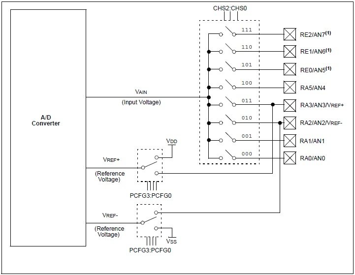
ADC Module Block Diagram – PIC18F4520
Selection of A/D Conversion Clock
The time for A/D Conversion per bit is defined as TAD and it requires minimum 12TAD to generate the 10-bit result. The time TAD is determined by the A/D Conversion Clock which is software selectable to following options.
- 2 TOSC
- 4 TOSC
- 8 TOSC
- 16 TOSC
- 32 TOSC
- 64 TOSC
- Internal RC oscillator of ADC Module
TOSC is the time period of the device clock usually provided by the crystal oscillator.
Care should be taken while selecting the A/D Conversion Clock, such that the clock should provide the minimum TAD(1.6μS) required for the correct A/D Conversion. So refer the following table before setting the ADC clock.
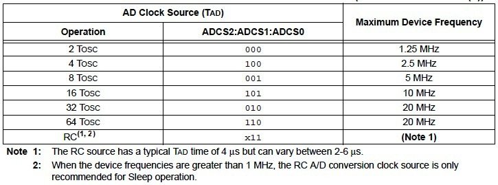
ADC Clock Selection Table – PIC18F4520
Program:
//Author : Palak Patel
//Contact No:9173211683
//Title:ADC
//Platform: PIC18F4520
//Software MPLAB
#include<p18f4520.h>
//#pragma config OSC =INTIO67
//#pragma config FCMEN = OFF
//#pragma config IESO = OFF
//#pragma config PWRT = OFF
//#pragma config BOREN = OFF
//#pragma config WDT = OFF
//#pragma config PBADEN = OFF
//#pragma config LPT1OSC = OFF
//#pragma config MCLRE = ON
//#pragma config STVREN = OFF
//#pragma config LVP = OFF
//#pragma config XINST = OFF
void cmd(unsigned char);
void dat(unsigned char);
void Delay_ms(unsigned char);
void main()
{
unsigned char temp[] = "TEMP",tdata[4],i,k;
unsigned int x=0,y,c=0x100,z,x1;
float p,tmpr,f;
TRISA=0x01;
TRISC=0x00;
cmd(0x01); //Clear Lcd
cmd(0x02); //4 Bit Specification
cmd(0x28); //4 Bit specification
cmd(0x0c);
cmd(0x80); //Cursor starting point
cmd(0X06);
i=0;
while(temp[i]!='\0')
{
dat(temp[i]);
i++;
}
cmd(0xC1); //Position second line 2nd character
ADCON1=0x0E;
ADCON0=0x00;
ADCON2=0x9C;
ADCON0bits.ADON = 1;
while(1)
{
ADCON0bits.GO=1;
while(ADCON0bits.GO==1);
x=ADRESH;
y=ADRESL;
z=(x*c)+y;
f=(z*(float)4.8875);
x1=(int)f;
tdata[3] = (x1/1000)%10 + 48;
tdata[2] =(x1/100)%10 + 48;
tdata[1] = (x1/10)%10 + 48;
tdata[0] = x1%10 + 48;
cmd(0xC3);
dat(tdata[3]);
dat(tdata[2]);
dat(tdata[1]);
dat(tdata[0]);
}
}
void cmd(unsigned char k)
{
PORTC &=0x0F;
PORTC |=(k & (0xF0));
PORTC |=(2<<0);
Delay_ms(2);
PORTC=PORTC & 0xFC;
Delay_ms(20);
PORTC &=0x0F;
PORTC |=((k<<4) & (0xF0));
PORTC |=(2<<0);
Delay_ms(20);
PORTC=PORTC & 0xFC;
Delay_ms(20);
}
void dat(unsigned char k)
{
PORTC &=0x0F;
PORTC |=(k & 0xF0);
PORTC |=(3<<0);
Delay_ms(20);
PORTC=PORTC & 0xFD;
Delay_ms(20);
PORTC &=0x0F;
PORTC |=((k<<4) & (0xF0));
PORTC |=(3<<0);
Delay_ms(20);
PORTC=PORTC & 0xFD;
Delay_ms(20);
}
void Delay_ms(unsigned char p)
{
unsigned int i,j;
for(i=0;i<p;i++)
{
for(j=0;j<20;j++);
}
}
Simulation:
For Basic Electronics Kindaly follow this Link:


